这篇笔记摘自Professional CUDA C Programming:
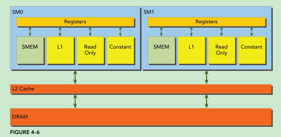
Global memory loads/stores are staged through caches, as shown in Figure 4-6. Global memory is a logical memory space that you can access from your kernel. All application data initially resides in DRAM, the physical device memory. Kernel memory requests are typically served between the device DRAM and SM on-chip memory using either 128-byte or 32-byte memory transactions.
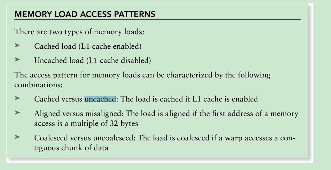
All accesses to global memory go through the L2 cache. Many accesses also pass through the L1 cache, depending on the type of access and your GPU’s architecture. If both L1 and L2 caches are used, a memory access is serviced by a 128-byte memory transaction. If only the L2 cache is used, a memory access is serviced by a 32-byte memory transaction. On architectures that allow the L1 cache to be used for global memory caching, the L1 cache can be explicitly enabled or disabled at compile time.
An L1 cache line is 128 bytes, and it maps to a 128-byte aligned segment in device memory. If each thread in a warp requests one 4-byte value, that results in 128 bytes of data per request, which maps perfectly to the cache line size and device memory segment size.
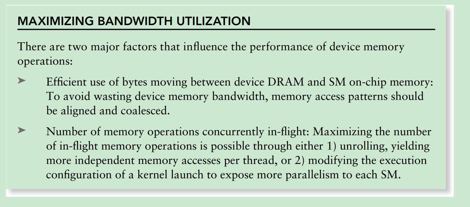
There are two characteristics of device memory accesses that you should strive for when optimizing your application:
➤ Aligned memory accesses
➤ Coalesced memory
Aligned memory accesses occur when the frst address of a device memory transaction is an even multiple of the cache granularity being used to service the transaction (either 32 bytes for L2 cache or 128 bytes for L1 cache). Performing a misaligned load will cause wasted bandwidth.
Coalesced memory accesses occur when all 32 threads in a warp access a contiguous chunk of memory.
Memory store operations are relatively simple. The L1 cache is not used for store operations on either Fermi or Kepler GPUs, store operations are only cached in the L2 cache before being sent to device memory. Stores are performed at a 32-byte segment granularity. Memory transactions can be one, two, or four segments at a time. For example, if two addresses fall within the same 128-byte region but not within an aligned 64-byte region, one four-segment transaction will be issued (that is, issuing a single four-segment transaction performs better than issuing two one-segment transactions).


